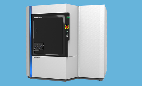
PHI Genesis
XPS and HAXPES combined in an automated multi-technology platform
High-tech products such as semiconductors or solid-state batteries today consist of very complex combinations of materials. XPS and HAXPES provide the necessary information to understand the properties and behaviour of these materials. Other important tasks include defect analysis and the testing of cleaning processes.
With PHI Genesis, ULVAC-PHI has integrated its highly successful XPS systems into one platform. XPS & HAXPES – surface analysis with two different excitation sources:
- XPS has an information depth of approx. 5nm.
- HAXPES has an information depth of about 15nm
The key technology in all PHI systems is the scanning X-ray source. It enables XPS analysis with very small beam diameters and at the same time a high-count rate. The scanning X-ray source is also the technology behind the so-called SXI imaging. SXI imaging allows imaging of your surface with the scanning X-ray beam and thus sample navigation as you are used to from an SEM.
Further System Benefits
- Easy Operation & Multi-technique Options
- High Performance Large & Micro Area XPS Analysis
- High Speed & Non-Destructive Depth Profiling
- Fully Automated with Sample Parking
- Hard X-ray Cr Kα source for HAXPES
- Comprehensive solution for batteries, semiconductors, organic devices and other applications

Application Areas

– Blog –