AFM-in-SEM method for failure analysis of bipolar junction transistors (BJTs)

Performing a professional failure analysis

Are you working in the semiconductor industry and looking for insights into the factors that lead to Bipolar Junction Transistor (BJT) failures?

Consider using the AFM-in-SEM method for failure analysis. This approach can provide helpful insights.

Perform failure analysis with NenoVision's LiteScope AFM tool, conveniently integrated into your SEM. This tool provides accurate and reliable results and ensures that your analysis is of the highest quality.

Benefits of fault analysis with LiteScope
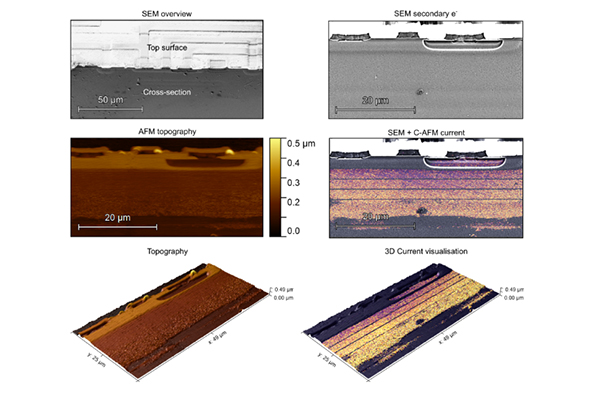
  • Focused Ion Beam (FIB) etching as an alternative to chemical etching for SEM contrast (for sample preparation).
  • Fast and easy ROI identification in SEM
  • Conductivity mapping under in-situ conditions (Conductive AFM is independent of SEM material contrast and provides a high-resolution map of the local conductivity of the sample).
Cross-section of a Bipolar Junction Transistor (BJT) - Analysis after FIB etching

Image: Cross-section of a Bipolar Junction Transistor (BJT) - Analysis after FIB etching

Sample courtesy of David Pléha, ON Semiconductor

BJT's and their weak points

Semiconductors are the backbone of modern electronic devices and systems. Bipolar transistors, especially bipolar junction transistors, have proven to be indispensable components in this context.

However, anyone involved in the manufacture, design, or application of BJTs knows that they are not infallible. Manufacturing errors, material defects, design problems and environmental influences can cause a transistor to not perform as expected or to fail prematurely. This is where failure analysis comes in.

Failure analysis is a critical process for understanding the causes of bipolar transistor malfunction or failure.

Extend the 2D SEM image to 3D and thus improve the material contrast in the SEM.

What are the benefits of performing a professional failure analysis?

  • Improve your components
  • Optimise your manufacturing processes
  • Increase your overall semiconductor device performance and reliability
  • Get longer-lasting and higher-performing electronic devices
  • Reduce costs
  • Minimise downtime