LiteScope
A unique AFM-in-SEM tool for multimodal in-situ correlative sample analysis
AFM-in-SEM
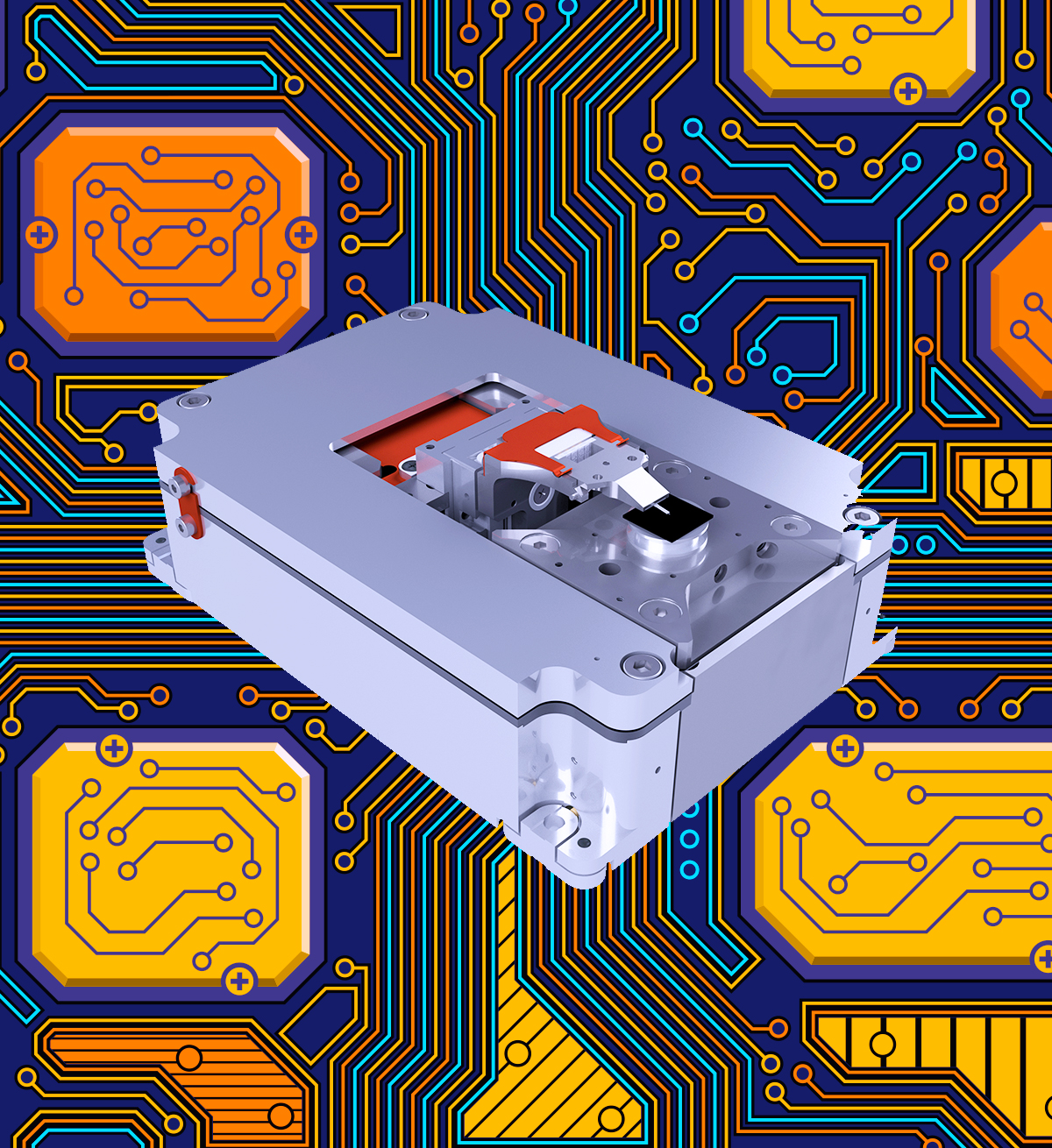
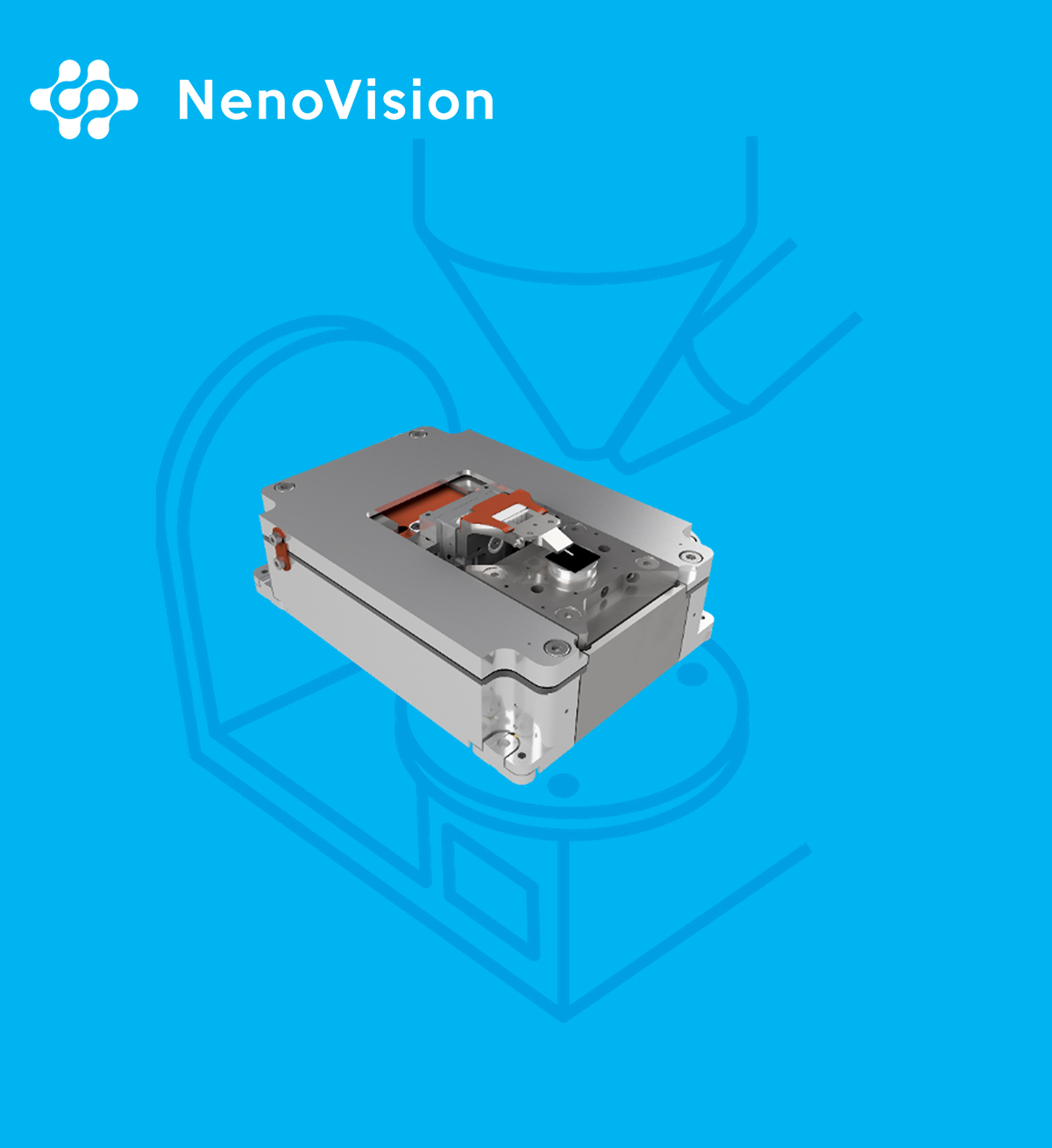
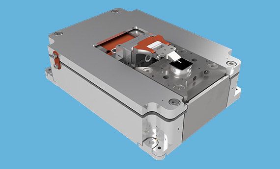
The Nenovision LiteScope™ is a compact Atomic Force Microscope designed for easy integration into Scanning Electron Microscopes.
Merging the strengths of AFM and SEM gives you the best of the two leading imaging techniques. It opens the door to completely new possibilities in the field of in-situ complex sample analysis. Successful applications have been a proof of the LiteScope™ in the fields of Material Science, Semiconductors, Life Science and Nanostructures.
CPEM which stands for Correlative Probe and Electron Microscopy allows the simultaneous detection and acquisition of signals from the LiteScope™ and the SEM. During scanning, the SEM electron beam points close to the AFM tip with a constant offset. They both remain static, while the sample is moving thanks to the LiteScope’s piezo scanner. This way, data from AFM and SEM microscopes can be acquired at the same time, in the same place, and under the same conditions.
The scan head was designed to fit into most SEM systems. It is easy to mount and compatible with SEM accessories like FIB, GIS and EDX. The self-sensing probes do not require optical detection or a complicated adjustment of a laser.
Further System Benefits
- Complex sample analysis: Simultaneous acquisition of data from SEM and AFM, and their seamless correlation into 3D images
- In-situ conditions: All measurements are done at the same time, at the same place, and under the same conditions, no risk of sample contamination
- Precise localization of the region of interest
- Enhancement of SEM capabilities

Application Areas
Successful applications of the LiteScope™ and CPEM have been made in the field of Material Science, Life Science, Semiconductors and Nanostructures.
Complex and correlative sample analysis
Cutting-edge CPEM technology allows the simultaneous acquisition of AFM and SEM data and their seamless correlation.
In-situ sample characterization
In-situ conditions inside the SEM ensure sample analysis at the same time, in the same place and under the same conditions.
Precise localization of the region of interest
Extremely precise and time-saving, the SEM navigates the AFM tip to the region of interest, enabling it to be located quickly and easily.
Additional Equipment

External nanoindentation module
The nanoindentation module enables micromechanical experiments to be performed while observing the specimen with superb SEM magnification and analyzing the indented specimen with sub-nanometer resolution using LiteScope.

NenoCase and digital camera
Use LiteScope as a stand-alone AFM in ambient conditions or under different atmospheres and navigate the AFM probe precisely with our digital camera.

Sample rotation module
The module is extremely useful for FIB milling procedures followed by an AFM analysis. It also allows the simultaneous mounting of several samples into the SEM chamber and the performing of their AFM and SEM correlative measurements without opening the chamber.
– Blog –