Exclusive Workshop at IKTS Dresden – 11 September 2025
“LiteScope AFM-in-SEM: Pushing the Boundaries of Semiconductor Failure Analysis and Material Characterisation”

We are pleased to invite you to our upcoming workshop ‘LiteScope AFM-in-SEM: Pushing the Boundaries of Semiconductor Failure Analysis and Material Characterisation’.
Please note that the number of participants is limited to 25.
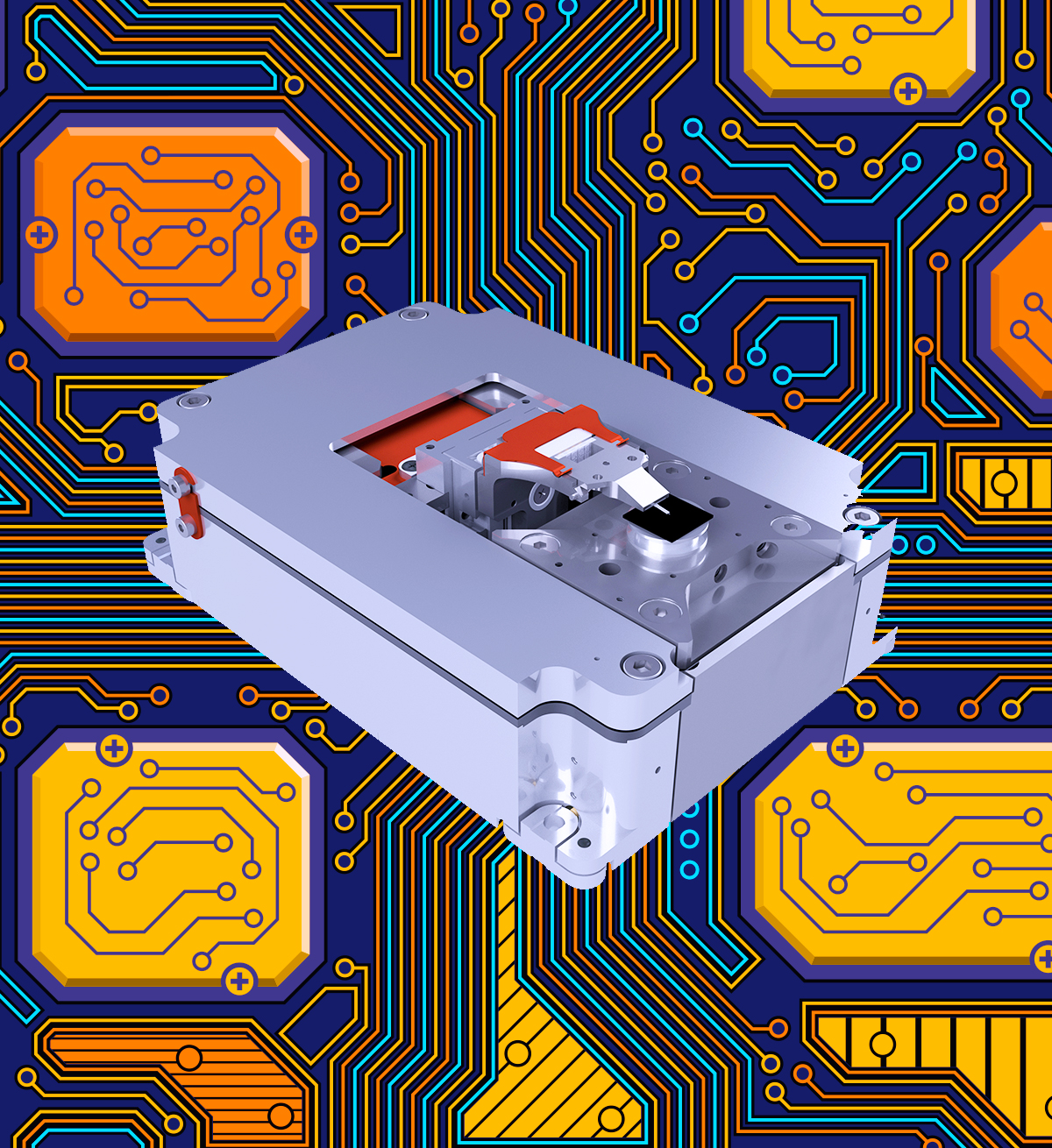
LiteScope is an innovative AFM-in-SEM tool, built for researchers pushing the limits of material science. Through its correlative CPEM mode, it enables simultaneous acquisition of morphological, electrical, mechanical, and magnetic data, directly inside your existing SEM environment.
Designed for both academic labs and industrial R&D, LiteScope enhances existing workflows while revealing hidden behaviours in devices and materials, previously impossible to discover with traditional tools. From failure analysis of semiconductor devices to battery materials characterisation, LiteScope AFM-in-SEM continues to reveal what others can’t.

Why attend?
“As semiconductor devices shrink and material architectures become more advanced, traditional failure analysis tools often fall short. That’s why I’d like to personally invite you to our upcoming AFM-in-SEM workshop at Fraunhofer IKTS in Dresden, where we will demonstrate how LiteScope enables precise, site-specific in-situ analysis directly inside the SEM.
This hands-on event will showcase how our integrated approach uniquely correlates topography, electrical, and mechanical properties – streamlining your workflow and delivering high-impact insights for semiconductor failure analysis and advanced materials research. Live demo will be included, to see the full workflow in action!”
 Jan Neuman, NenoVision
Grab your spot here & now
In-situ/correlative microscopy
In-situ microscopy refers to the technique of observing and analysing materials or samples in their native environment without removing or altering them during the measurement process. This method is critical for R&D as it provides real-time, undisturbed observations, enabling accurate studies of dynamic processes such as reactions, phase transitions, or failure mechanisms in materials.
Correlative microscopy combines different imaging techniques (such as SEM and AFM) to capture complementary data on the same sample, offering a comprehensive view of both structure and function. In R&D, this approach is invaluable for linking topographical, electrical, and mechanical properties, helping researchers gain deeper insights into complex materials and systems.

Complex and correlative sample analysis
Cutting-edge CPEM technology allows the simultaneous acquisition of AFM and SEM data and their seamless correlation.
True site-specific failure analysis
Navigate directly to specific vias, transistors, or doped layers and perform localised electrical AFM analysis with nanoscale precision.
Reduce time and cost per analysis
Eliminate time-consuming sample transfers and redundant tool usage – streamline failure localisation into a single workflow within your existing SEM environment.
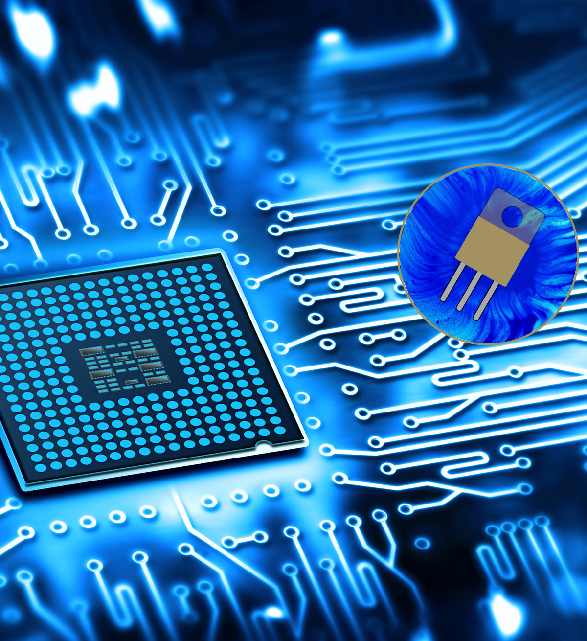
Application Area
– Blog –