Subnanometer accuracy for the chip industry: TOF-SIMS in focus

May 20, 2025

Subnanometer accuracy for the chip industry

TOF-SIMS in focus
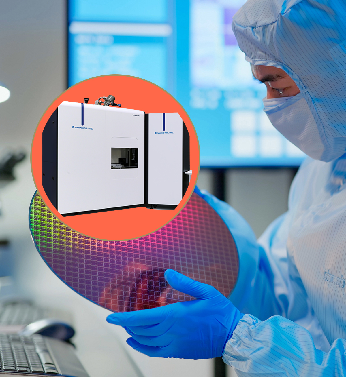
The combination of time-of-flight secondary ion mass spectrometry (TOF-SIMS) and tandem mass spectrometry enables high-resolution, three-dimensional imaging of the chemical composition of surfaces. This is particularly relevant for the analysis of (sub-)monolayer coatings in semiconductor manufacturing.

What is TOF-SIMS Tandem MS Imaging?

TOF-SIMS (Time-of-Flight Secondary Ion Mass Spectrometry) is a technique in which the surface of a material is bombarded with an ion beam. Secondary ions are extracted from the surface, which are then analysed according to their mass-to-charge ratio.
Tandem MS (MS/MS) extends this method by additionally fragmenting and re-analysing selected ions. This provides structural information about molecules, not just their mass.

 Application in the semiconductor industry

  • Analysis of ultra-thin layers:
    In semiconductor production, extremely thin layers (often only a few atomic layers thick) are applied to wafers. TOF-SIMS can chemically and spatially resolve these layers to recognise impurities or doping, for example.

  • 3D depth profiling:
    TOF-SIMS can create a three-dimensional chemical profile by controlled ablation of the surface (sputtering). This is crucial for understanding the distribution of materials in transistor structures, for example.

  • Molecular identification:
    Tandem MS can be used to differentiate between molecules with the same mass but different structures - such as isomeric compounds or degradation products of process chemicals.

  • Error analysis and quality assurance:
    If a component fails, TOF-SIMS can help to identify residues, contamination or process errors - often down to the molecular level.

  • Process optimisation:
    By precisely analysing layer compositions and interfaces, manufacturing processes can be specifically adapted to improve yield and reliability.

Use of the PHI nanoTOF 3

Simultaneous acquisition of MS¹ and MS² data

Speeding up your  analysis

High spatial resolution (<100 nm)

Ideal for modern micro- and nanostructures

Automated sample handling

Particularly helpful for serial analyses in production

– Blog –

Learn more about this product...

Go to Top