ICSPI nGauge AFM
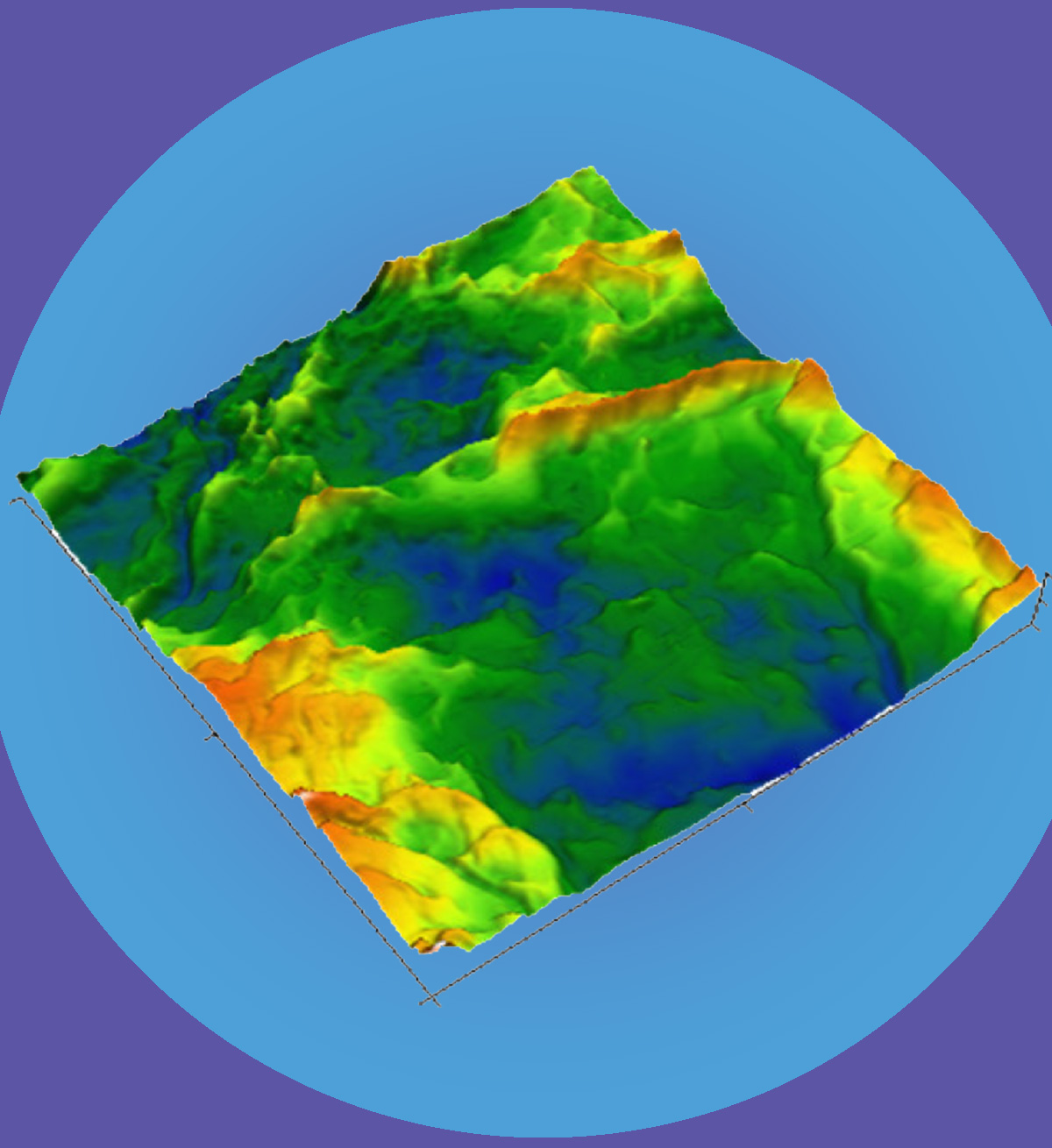
3D images with nanoscale resolution
The ICSPI nGauge is a benchtop AFM tool based on the patented AFM-on-a-Chip technology. In this AFM all scanners and sensors are integrated into a single 1 x 1 mm2 CMOS-MEMS chip and therefore nanoscale imaging has never been easier.
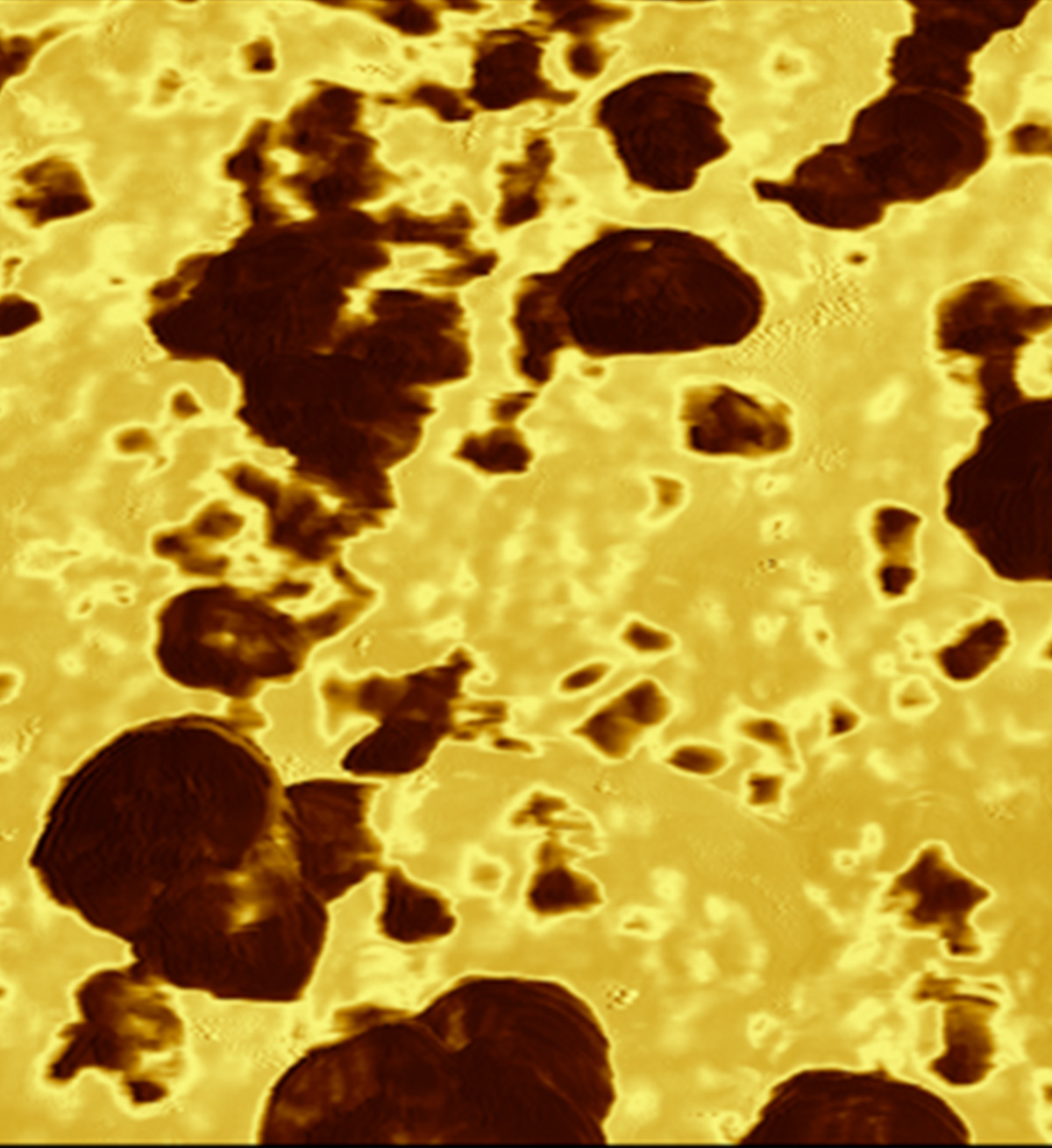
Atomic Force Microscopy (AFM) is one of the most used surface science techniques to investigate topography, surface roughness and thickness of coatings on different substrate materials. A very sharp tip or cantilever is moving across the surface giving height and mechanical information on the nanoscale. The nGauge is working in the so-called tapping mode providing very long cantilever lifetimes and 1000+ scans.
The ICSPI AFM-on-a-Chip approach resulted in an alignment-free, laser-less and cost-effective AFM tool.
The nGauge AFM offers a simple benchtop set-up and plug-and-play operation providing first results within a few minutes.

Further System Benefits
- Fast – Collect data in less than 2 minutes
- Easy to use – collect scans in 3 clicks
- Benchtop – small footprint and low weight (500 g)
- Laser-less system – no calibration/alignment
- Easy transportation – comes in a compact suitcase
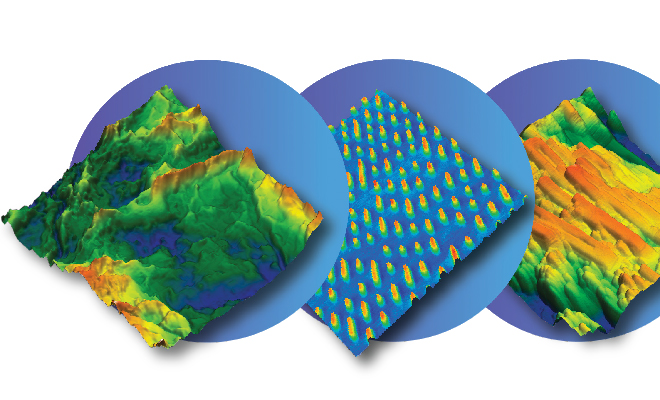
Application Areas
Very fast Plug- and play operation
Connect the nGauge to the power line and the computer. After startup of the software there are three clicks to start a measurement: frequency sweep, automatic approach and starting the scan.
Laser-less setup
No time-consuming calibration necessary since the nGauge is operating with self-sensing tips and automatic approach of the sample to the tip.
CMOS MEMS technology
All sensors and actuators are integrated in an CMOS MEMS chip. This resulted in a very compact system with a small footprint to fit in any laboratory environment.
– Blog –